Programmer for microcontrollers
This week we fabricate a circuit board for programming microcontrollers with a microcontroller. The circuit diagram is shown as follow. Because there is not much challenge or novelty in making the board itself, I spend most my energy and time in understanding the circuit and learning about microcontrollers.
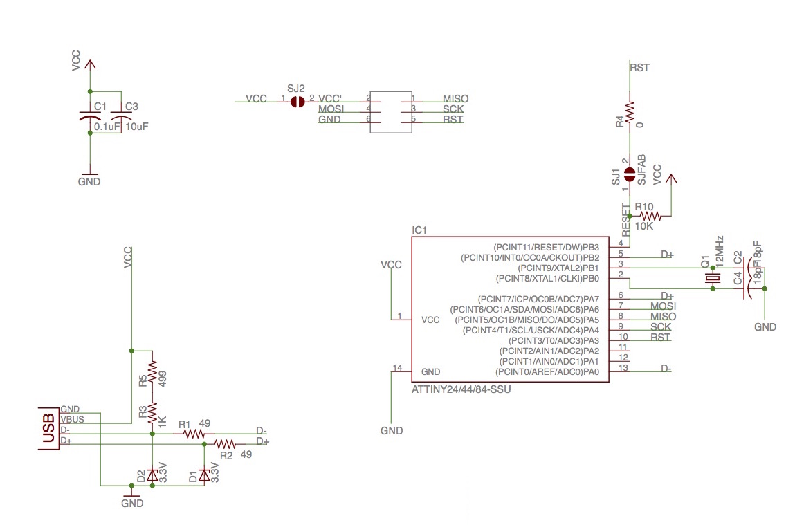
First thing I got puzzled was why we need a programmer to program a microcontroller instead of programming it with a computer through USB directly. Then I learned that most microcontrollers can't communicate via USB (which only have one data channel), instead they use SPI (Serial Peripheral Interface) to communicate. In the SPI interface, there are six ports: VCC, GND, SCK, MOSI, MISO and reset. The first two are just power supply and ground, the third port is used to synchronize the clock between the master (programmer) and the slave (microcontroller to be programmed). MOSI and MISO stand for master-out-slave-in and master-in-slave-out, which are the two way data channels. After the programmer board is programmed, then it takes in data from the USB and translate it into language that can be understood by SPI interface on the microcontroller.
The circuit shown above consist of four blocks. The first block on the top-left looks like a simple filter which makes the power supply more stable as high frequency noise is directly shorted to the ground. The second block on the top-right is simply showing SPI interface. Jumper wire SJ1 and SJ2 are connected when the programmer is being programmed by other programmers; SJ1 supply the power to this board and SJ2 send a low input to the board to reset it. Once programming finished, SJ1 and SJ2 are taken out as the power is supplied by USB port and reset no longer needed and locked at high state.
The third block on the bottom left is used to translate USB signal to data input for the programmer. USB consists of four lines: 5V power supply, ground, D+ and D-. D+ and D- are used to transmit data, a digital '1' is transmitted by pulling D+ over 2.8V with a 15K ohm resistor pulled to ground and D- under 0.3V with a 1.5K ohm resistor pulled to 3.6V. ‘0’ on the other hand is a D- greater than 2.8V and a D+ less than 0.3V with the same appropriate pull down/up resistors. After the circuits in the third block, '1' state is represented by both D+ and D- is at high state and '0' is represented by a high D- and low D+.
The last block on the bottom right is simply a ATtiny microcontroller with power supply on the left and 20Mhz crystal oscillator on the right. D+, D- and SPI wires are connected with input and output of the microcontroller.
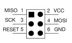
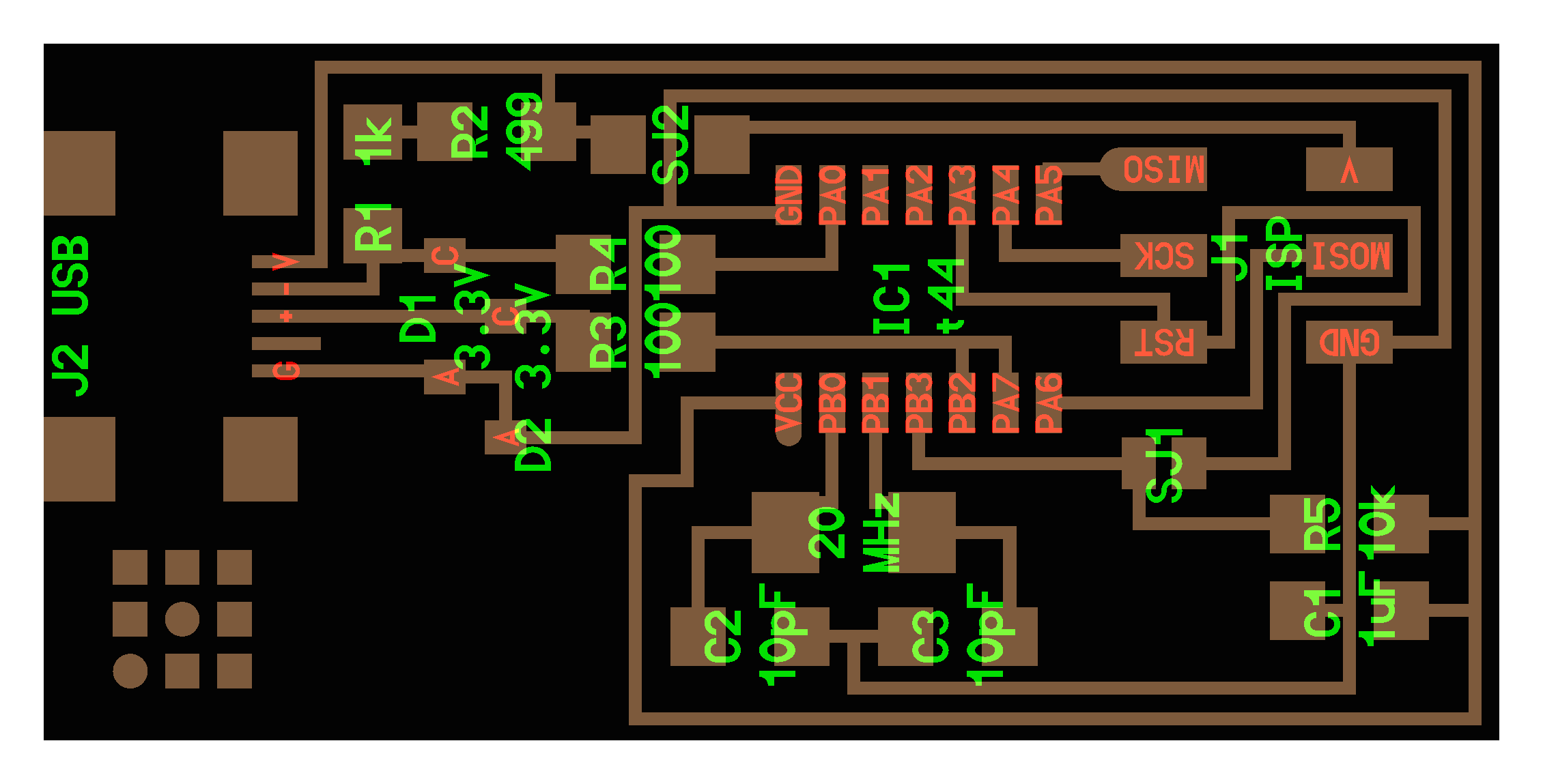
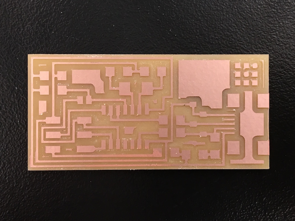
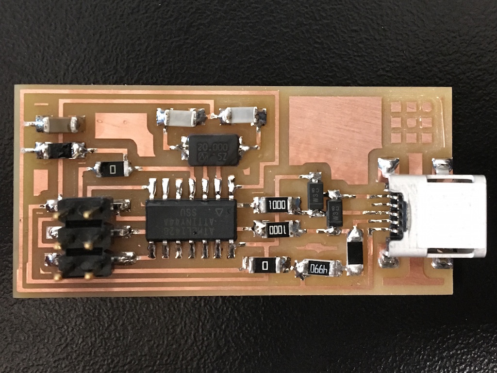
Layout diagram for the circuit and SPI illustration are shown above. We make the circuits with 1/64' end mill and cut the the board off with 1/32'. Then the board is stuffed and soldered, be careful with the direction of the diodes and IC chip (there is a small round dot on the IC to tell the direction). Because I had extensive experience with soldering, it didn't take much effort to populate the board.
For the testing and programming of the boarded. We first connect the board with another programmer through SPI interface. We tested the supply voltage to be around 5V and the programming was successful. Then I de-soldered the SJ1 and SJ2 resistor, plug the programmer onto computer USB, it was successfully recognized. At last, I made the cable for SPI interface for communicating with other board to be programmed.